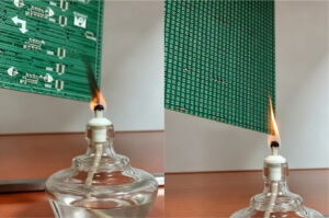
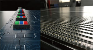
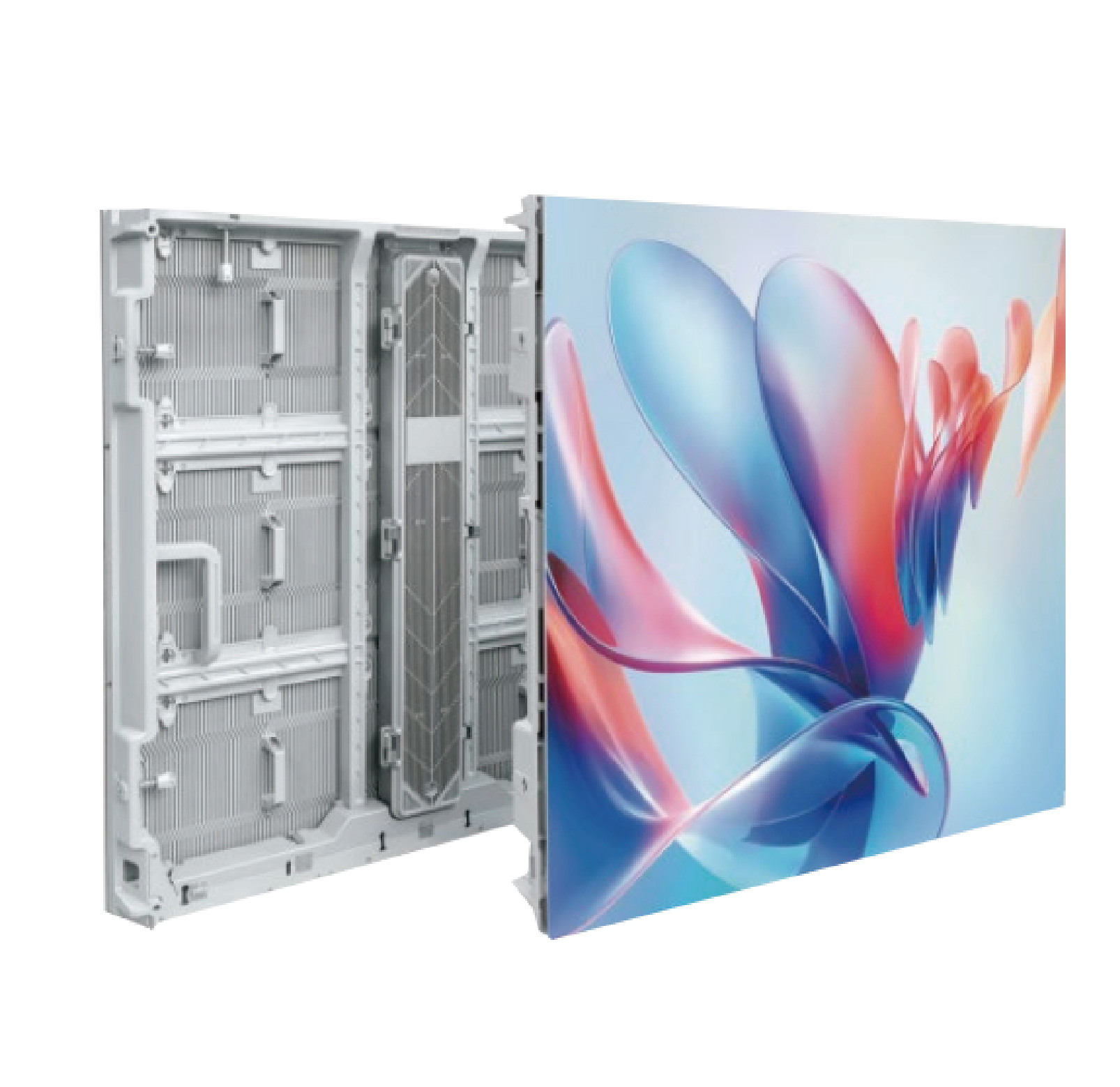
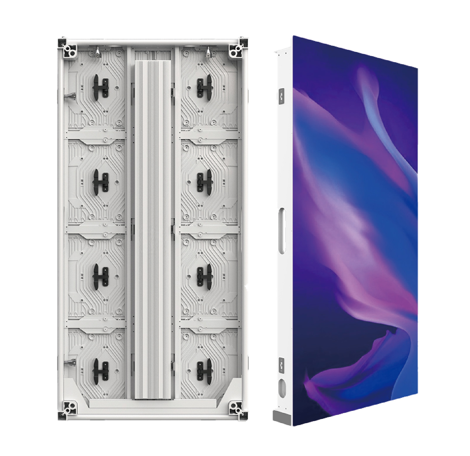
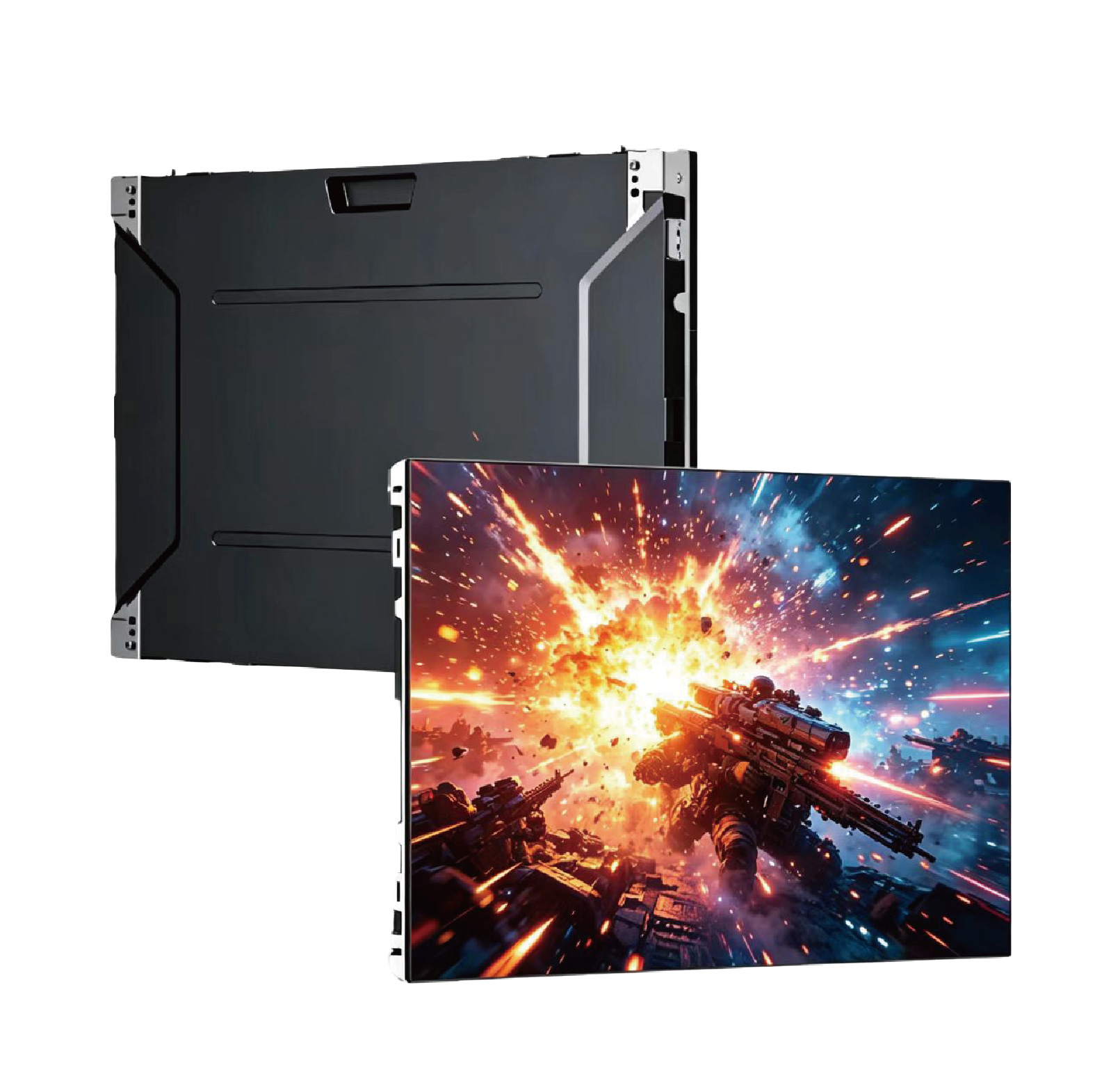
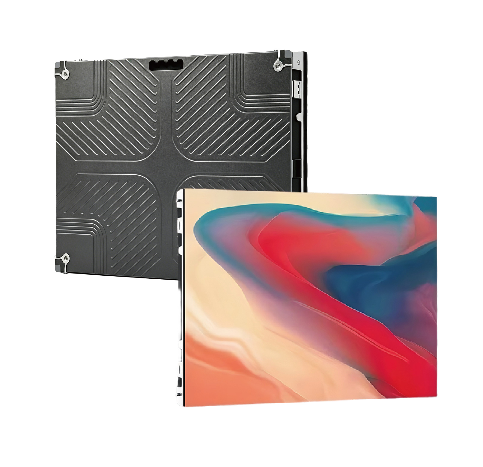
Vibration, impact and temperature fluctuation often cause pad peeling and dead pixels in LED displays. Our private‑mold PCB enhances solder‑pad reliability by adopting multi‑layer structure, thick substrate, enlarged copper pouring and flame‑retardant base material.
Core PCB Design Advantages|PCB
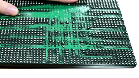
We use an 8‑layer, 1.6 mm flame‑retardant PCB. Each LED pin features 15 % larger copper‑pouring area than conventional boards, with reinforcement on every copper point. Expanded copper coverage strengthens bonding between solder pads and substrate to prevent pad drop under shock and vibration.
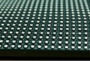
Building on copper‑pouring reinforcement, well‑positioned vias are added in design around each lamp‑pin copper zone. Dense metallized vias firmly anchor copper layers to the substrate for higher structural strength. They also improve heat dissipation and current conduction while releasing thermal stress from temperature cycling to prevent pad warping and cracking. Vias maintain safe spacing so pad integrity remains undamaged.
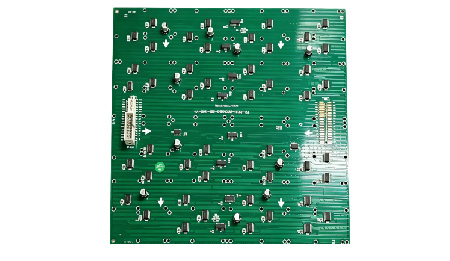
The multi‑layer layout optimizes power‑signal routing for better current capacity and signal stability. The 1.6 mm board delivers high rigidity against bending stress, and flame‑retardant material enhances long‑term operating safety.
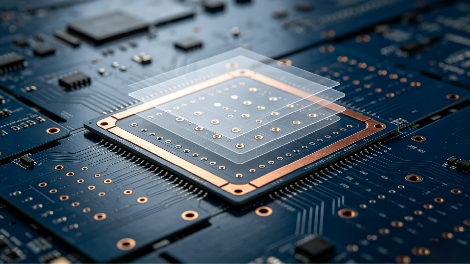
Application Value
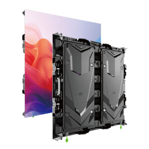
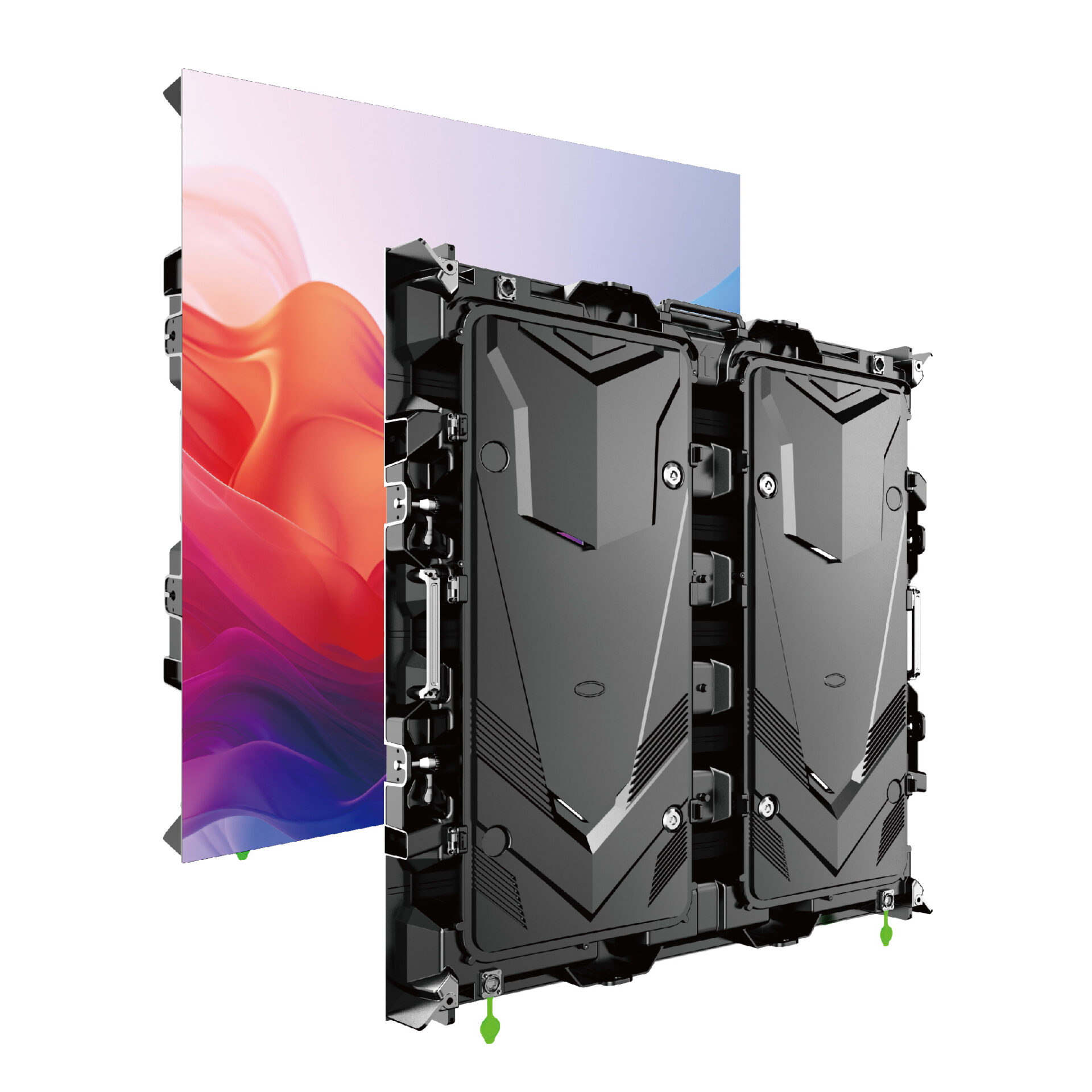
This PCB fits high‑turnover rental screens, wide‑temperature outdoor units and indoor fine‑pixel fixed installations, cutting hidden risks and project maintenance costs. The 8‑layer 1.6 mm flame‑retardant PCB with reinforced copper pouring fundamentally improves anti‑drop pad performance for reliable LED display projects.